 |
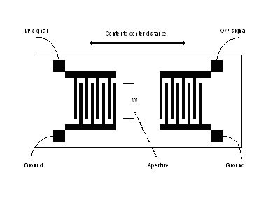
The SAW layout consists of two metal film inter-digital transducers
(IDT) bonding pads and a space between the IDT's. Lithium niobiate is used
for the substrate and devices are fabricated by photolithography.
|
|
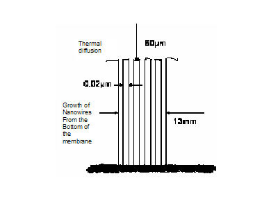
Palladium nanowires are placed between the IDT's.
Due to its high selectivity and resistance to poisoning, Palladium is chosen as
the nanowire material. The nanowires are created experimentally into a structured nanowire array.
|
|
|
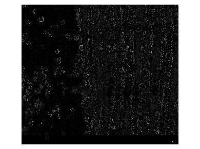
Effects of varying deposition potential on Palladium nanowire.
The electrodeposition was carried out from an aqueous solution
of 2 mM Pd(NO3)2 and 0.1 M HClO4 on a highly oriented pyrolitic
graphite surface. ). In the SEM pictures the gray matrix is identified as alumina,
light area is due to the presence of nanowires and the dark regions are identified with empty pores.
|

